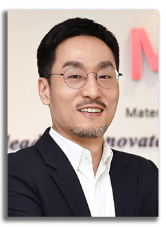
Click image for HiRes
Abstract
Electronic trap states are a critical yet unavoidable aspect of semiconductor devices, 20 impacting performance of various electronic devices such as transistors, memory devices, solar cells, and LEDs. The density, energy level, and position of these trap states often enable or constrain device functionality, making their measurement crucial in materials science and device fabrication. Most methods for measuring trap states involve fabricating a junction, which can inadvertently introduce or alter traps, highlighting the need for 25 alternative, less-invasive techniques. Here, we present a unique photo-Hall-based method to detect and characterize trap density and energy level while concurrently extracting key carrier properties, including mobility, photocarrier density, recombination lifetime, and diffusion length. This technique relies on analyzing the photo-Hall data in terms of “photo-Hall conductivity” vs. electrical conductivity under varying light intensities and 30 temperatures. We show that the photo-Hall effect, in the presence of traps, follows an astonishingly simple relationship — a hyperbola equation — that reveals detailed insights into charge transport and trap occupation. We have successfully applied this technique to P and N-type silicon as a benchmark and to high-performance halide perovskite photovoltaic films. This technique substantially expands the capability of Hall effect-based 35 measurements by integrating the effects of the four most common excitations in nature —electric field, magnetic field, photon, and phonon in solids — into a single equation and enabling unparalleled extraction of charge carrier and trap properties in semiconductors.
Click here to see all available video seminars.
Click here to go to the SPREE HOMEPAGE.
Brief Bio
Byungha Shin is Professor in the Department of Materials Science and Engineering (MSE), at Korea Advanced Institute of Science and Technology (KAIST) in Daejeon, Korea. Prof. Shin received B.S. in MSE from Seoul National University in 2000, M.S. in MSE from the University of Michigan in July 2002, and Ph.D. in Applied Physics from Harvard University in 2007. From May 2007 to March 2010, he was a post-doctoral researcher in the Department of MSE at Stanford University. From May 2010 until he joined KAIST in Feb 2014, he worked at IBM T. J. Watson Research Center as a post-doctoral researcher and a Research Staff Member. He also spent seven months from Aug 2018 to Feb 2019 as a visiting Professor at Columbia University. In his administrative roles, he served as the Associate VP of the Office of Student Life from 2021 to 2023 and has been the Director of the KAIST Global Leadership Center from 2021 to 2024. As of March 2024, he began serving as Department Head of MSE.
His past research experience includes the study of thin film growth kinetics and high-k dielectric materials for microelectronic applications. His current primary research interest is developing novel materials for energy applications with the current emphasis on hybrid perovskite optoelectronic devices (PV, LED, and radiation-detector), chalcogenide thin film solar cells, and photoelectrochemical water splitting and electrochemical nitrogen reduction.
He has published over 130 SCI journal papers, including Science (2020) and Nature (2019), and he has given over 100 invited talks at various academic institutes and international conferences. He was a recipient of “Scientist of the Month” and “100 Outstanding Research Achievements”, both by Ministry of Science and ICT of Korean Government in 2021, “The 2020 KASTian of the Year Award” by KAIST in 2020, and “KAIST’s Top 10 Research Achievements of 2019” by KAIST in 2019. In 2025, he was elected as a Fellow of The Korea Academy of Science and Technology.
