Abstract
For the past few years, we have been working to develop colloidal dispersions of nanocrystals, or inks, as precursor materials to fabricate mechanically flexible, light-weight photovoltaic devices (PVs). Our work has primarily focused on copper indium gallium selenide (and sulfide) (CIGS) and copper zinc tin sulfide (CZTS) with the goal of eliminating the use of high temperature, vacuum processing. We can make printed CIGS devices with power conversion efficiencies of just over 3% under AM 1.5 illumination without high temperature processing, on glass or plastic substrates. We can achieve just over 8% PCE by sintering the nanocrystal film with a high temperature (~500oC) selenization step. These efficiencies are not yet commercially viable, but demonstrate that nanocrystal inks have potential as a precursor material for printed light-weight flexible solar cells. The device efficiency is predominantly limited by poor electrical transport in the nanocrystal layer. Recently, the Sargent and Bawendi groups achieved >8% PCE in PbS nanocrystal devices processed at low temperature by judicious surface modification of the nanocrystals. We have also been examining various strategies to engineer CIGS nanocrystal surfaces to improve device performance, as weall as a different approach that enables nanocrystal sintering under ambient conditions called photonic curing. Photonic curing utilizes a high intensity, rapidly-pulsed broad-band light source to generate extremely high temperatures (up to 1000oC) in microseconds. Using this approach to process CuInSe2 nanocrystal absorber layers, devices with peak external quantum efficiencies (EQE) of just over 100% were made, consistent with the extraction of multiexcitons. Carrier multiplication (CM)—or multiexciton generation (MEG)—in these nanocrystal-based films was confirmed by transient absorption spectroscopy (TAS), and using TAS measurements on CuInSe2 nanocrystals with various size, the energy threshold for CM in the CuInSe2 nanocrystals was found to be 2.4 ± 0.2 times the nanocrystal optical gap with a CM efficiency of 36 ± 6%, which is similar to other types of nanocrystal quantum dot materials. The properties of the nanocrystal films and their relationship to the observed device efficiency will be presented, along with a discussion about how to further improve the efficiencies of nanocrystal-based devices.
Click here to see all available video seminars.
Click here to go to the SPREE HOMEPAGE.
Brief Bio
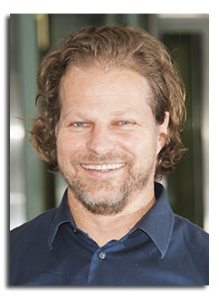
Brian A. Korgel is the T. Brockett Hudson Professor of Chemical Engineering at the University of Texas at Austin (USA) and works in the field of nanomaterials chemistry and complex fluids. He received his PhD from UCLA in 1997 and was a post-doctoral fellow at University College Dublin, Ireland until 1998 before joining the faculty at UT Austin. He has been Visiting Professor at the University of Alicante in Spain as a Senior Fulbright Fellow, Visiting Professor at the Université Josef Fourier in France and Distinguished Visiting Professor at the Chinese Academy of Sciences in Beijing. He directs the Industry/University Cooperative Research Center for Next Generation Photovoltaics, has co-founded two companies, Innovalight and Piñon Technologies, and now serves as an Associate Editor for Chemistry of Materials. He, has published more than 200 papers and has received various honors including the Professional Progress Award from the American Institute of Chemical Engineers (AIChE) and the ISHA Roy-Somiya Medal, and is a Fellow of the American Association for the Advancement of Science (AAAS).
